


US, Japan and China in Gallium Oxide Semiconductor Race
By Brian Wang

The US, China and Japan are working on research and development in gallium oxide crystal growth and productionizing gallium oxide chips. The Gallium oxide chips can have a voltage resistance value 3 times higher and power consumption reduced by 60%.
The power semiconductor market, sometimes called power electronics, is a large and important business that often flies under the radar. In total, the power electronics market, including discretes and modules, was worth $23.8 billion in 2023, and is expected to grow to $35.7 billion by 2029, according to the Yole Group, a market research firm. The work on Gallium Oxide is still early and there some projections if could get to about $1 billion in business around 2030, which would be about 3% of the total power semiconductor market.
Power semiconductors are used in nearly every electronic system. Power semiconductors supply and control electricity used to run motors and charge batteries by converting electric power from AC to DC and adjusting voltages to appropriate levels.
In addition, these devices are used to control the flow of electricity in systems, while reducing the power losses during operation. And unlike conventional chips like AI devices and processors, power semis can withstand higher voltages and currents with lower losses in systems.
Power semiconductors are categorized into different product families, including power MOSETs, IGBTs, GaN power devices and SiC MOSFETs. There are many other power device families.
Gallium oxide has a band gap of 4.8 eV, with a critical field value of 8 MV/cm. This band gap is 3,000 times that of silicon, more than 8X that of SiC, and more than 4X that of GaN. Theoretically ultra-wide band gap semiconductor devices based on gallium oxide can withstand higher voltages with a lower resistance than GaN, SiC, and, of course, silicon.
The problem? There are several challenges with gallium oxide, preventing the devices based on the technology from moving into production. Gallium oxide has poor thermal conductivity, which could cause a device to overheat. In addition, there is no intrinsic p-type doping technique for gallium oxide.
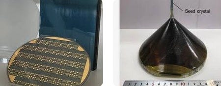
Gallium oxide wafers are easier to produce versus GaN (Gallium Nitride) and SiC (silicon Carbide) substrates. But today, gallium oxide is produced on 2-inch wafers, with 6-inch (150mm) substrates in the works. It’s difficult to produce cost-effective devices on smaller wafer sizes.
Virginia Tech, U.S. Naval Research Laboratory and NCT presented a paper that represents a possible breakthrough for gallium oxide in late 2024. Researchers built a lateral Ga2O3 junction-gate field-effect-transistor (JFET), employing high p-doped NiO for E-mode operation, and hybrid-drain structures for electric field management.
Japan is a leader in gallium oxide. Two Japanese companies, Flosfia and NCT, are working on the technology.
In 2023, Flosfia and JSR developed a new iridium-based film deposition material as a solution for mass production of iridium gallium oxide. This material enabled the world’s first p-type power semiconductor developed using a corundum-type gallium oxide compound. This device is still in R&D.
NCT, meanwhile, has demonstrated several gallium oxide power devices, which are in R&D. The company also sells 2-inch gallium oxide wafers. NCT is working on 6-inch wafers with plans to move into small-scale production by 2026.
Gallium oxide chips offer several significant advantages over traditional silicon-based semiconductors:
Higher conductivity: Gallium oxide-based chips are five times more conductive than silicon counterparts, leading to reduced energy losses in data centers.
Higher voltage operation: These chips can handle higher voltages, making them ideal for demanding data center environments.
Higher temperature operation: Gallium oxide components can operate efficiently at higher temperatures, reducing the need for extensive cooling systems.
Higher frequency operation: This enables faster data processing and transmission, crucial for AI and advanced computing applications.
Ultra-wide bandgap: Gallium oxide has a bandgap of 4.8 eV, which is 3,000 times that of silicon, more than 8X that of SiC, and more than 4X that of GaN.
Compact and efficient: Gallium oxide semiconductors offer advantages in high-voltage resistance, smaller size, and less energy consumption in power transmission
China:
MIG Semiconductor Company successfully produced 4-inch gallium oxide wafers in December 2024.
MIG is building China's first integral production line, combining crystal growth, processing, and performance testing, expected to be completed by the end of 2025.
Fujia Gallium, recently broke ground on China’s first 6-inch gallium oxide monocrystalline and epitaxial wafer growth line.
Keep reading with a 7-day free trial
Subscribe to next BIG future to keep reading this post and get 7 days of free access to the full post archives.