
NVIDIA Chip Roadmap: B200, Rubin and Beyond Versus Tesla Dojo 2, 3 and 4
By Brian Wang

NVIDIA's chip roadmap progresses from the B200, part of the Blackwell architecture, to the Rubin architecture, with hints of potential "ultra" chips or new architectures in the future.
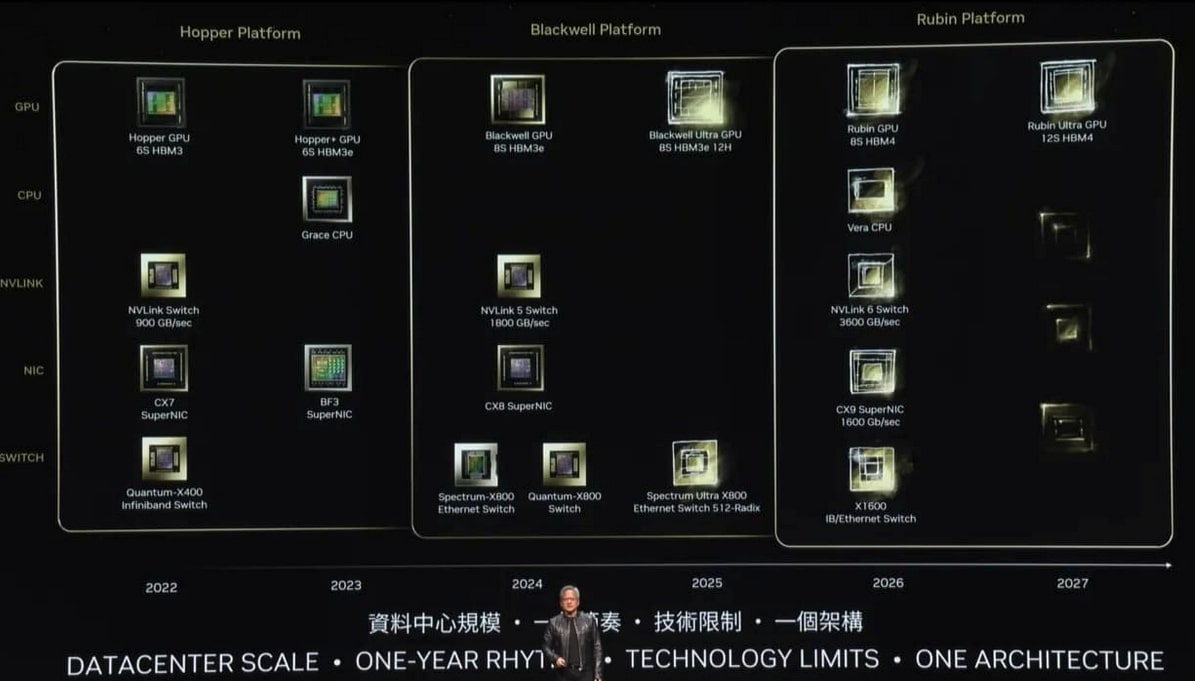
The next generation Nvidia Rubin chip is expected late in 2025 and their should be an Ultra variant of the Blackwell chip.
At the late 2024 All in Summit Elon said:
Dojo 2 Chip: Elon Musk expected the Dojo 2 chip to be in high volume production by late 2025. This means that by the end of 2025, Tesla anticipates having the Dojo 2 AI training chip and its associated systems widely available and operational at scale, competitive with advanced systems like NVIDIA’s B200.
Dojo 3 Chip: Musk mentioned the Dojo 3 chip in the context of late 2026, indicating that its performance would be critical to assessing the long-term success of the Dojo project. He suggested that Tesla would need to evaluate Dojo 3 around that time to determine if the Dojo initiative would be "really good and an ongoing success."
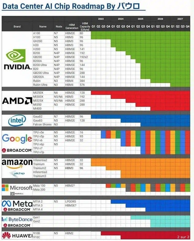
There is compiled information on chip roadmaps and expected amounts of memory. This also shows that scaling HBM memory or alternative memory is needed to continue scaling artificial intelligence data centers.
Here's a detailed breakdown:
B200 (Blackwell Architecture)
Announced in March 2024 at NVIDIA's GTC keynote, the B200 is a high-performance GPU designed for AI and data center applications. It is fabricated on TSMC's 4NP node (an enhanced version of the 4N node). Key specifications include:
Power consumption: Up to 1000W.
AI compute performance: 9 petaFLOPS of FP4 precision.
This chip represents a significant leap in compute power and efficiency for AI workloads.
Rubin Architecture
The Rubin architecture is NVIDIA's next major step, expected to succeed Blackwell. It is anticipated to launch in late 2025 or early 2026 and will likely be fabricated on TSMC's 3nm process node.
This shift promises:
Increased transistor density.
Enhanced performance and power efficiency.
Specific specifications for Rubin are not yet publicly detailed
Beyond Rubin: Ultra Chips and New Architectures
Beyond Rubin, information becomes speculative. There is ultra chip variant and an entirely new architecture. These could involve even more advanced process nodes (e.g., 2nm) or novel architectural designs, though specifics remain unavailable at this time.
Expected Specifications Based on Reports and Analysis
Rubin Specifications
While exact specs for Rubin are not yet available, its use of TSMC’s 3nm process suggests:
Higher transistor density than Blackwell.
Improved performance-per-watt, critical for next-gen AI and compute tasks.
Ultra Chips and Beyond
No specific data exists for post-Rubin developments. However, trends suggest future chips could target even greater compute density
Tesla Dojo Roadmap: Dojo 2, Dojo 3, and Dojo 4
Tesla’s Dojo supercomputer is designed for AI training.
Here’s the expected roadmap:
Dojo 1 (Current Generation)
Uses the D1 chip, fabricated on TSMC’s 7nm process. It’s operational and supports Tesla’s AI efforts today.
Dojo 2
The next generation, often referred to as Dojo 2, is in development. Elon has talked about rivaling the B200.
Release Timeline: Late 2025 per Elon
These are further future iterations, with no specific release dates or specifications available. Given Tesla’s focus on advancing FSD, expect:
Incremental upgrades in chip performance.
Possible adoption of more advanced process nodes (e.g., 5nm or 3nm).
Placing Dojo 3 around 2026 and Dojo 4 in 2027-2028, though this is speculative.
Production Volume: TSMC’s Role and Investments
Both NVIDIA and Tesla rely on TSMC for chip fabrication, and production volume depends on TSMC’s wafer capacity, capital projects, and efforts to address packaging constraints. Here’s the breakdown:
Keep reading with a 7-day free trial
Subscribe to next BIG future to keep reading this post and get 7 days of free access to the full post archives.